Orin NX: Direct GPIO Access via Registers
It should be noted that GPIO configuration must normally be performed through pinmux files — this is the correct and safe approach. However, in some cases it may be necessary to control GPIOs directly. For example, you might need to configure a specific pin as an output and drive it using push-pull, or set it as an input and read its logic level (1 or 0).
In this example, we will first configure pin206 as an output and observe its output level changing. Then, we will switch the same pin to input mode and read the input value.
To begin, download the pinmux configuration for the Orin NX from the following link:
https://developer.nvidia.com/downloads/jetson-orin-nx-and-orin-nano-series-pinmux-config-template
Next, let’s find pin206 in the document:
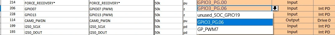
By default, the pin is configured as an input with a pulldown resistor.
We can also see that pin206 corresponds to SOC_GPIO19 or GPIO3_PG06.
These values will be useful later when locating the required registers in the TRM (Technical Reference Manual).
Next, we’ll need the Orin NX TRM. Download it from the following link:
https://developer.nvidia.com/downloads/orin-series-soc-technical-reference-manual/
To control the pin, we need the memory-mapped addresses of the following registers:
GPIO_G_ENABLE_CONFIG_06_0
GPIO_G_OUTPUT_CONTROL_06_0
GPIO_G_OUTPUT_VALUE_06_0
GPIO_G_INPUT_06_0
PADCTL_G4_SOC_GPIO19_0
Using the datasheet, we can find the addresses to which the registers are mapped.
To do this, we add the base address and the corresponding offset:
GPIO_G_ENABLE_CONFIG_06_0, base: 0x02200000 + offset: 0x140c0 = 0x022140c0
GPIO_G_OUTPUT_CONTROL_06_0, base: 0x02200000 + offset: 0x140cc = 0x022140cc
GPIO_G_OUTPUT_VALUE_06_0, base: 0x02200000 + offset: 0x140d0 = 0x022140d0
GPIO_G_INPUT_06_0, base: 0x02200000 + offset: 0x140c8 = 0x022140c8
PADCTL_G4_SOC_GPIO19_0, base: 0x02214000 + offset: 0x080 = 0x02434080
Knowing the register addresses, we can directly control the selected pin.
1)Let’s start by configuring pin206 as an output in push-pull mode.
In the PADCTL_G4_SOC_GPIO19_0 register, specify that pin206 is used as a GPIO with no pull-up or pull-down resistors enabled:
sudo busybox devmem 0x02434080 w 0x00
In the GPIO_G_ENABLE_CONFIG_06_0 register, enable pin206 as a GPIO output:
sudo busybox devmem 0x022140c0 w 0x3
In the GPIO_G_OUTPUT_CONTROL_06_0 register, set pin206 to DRIVEN (under control):
sudo busybox devmem 0x022140cc w 0x0
Finally, using the GPIO_G_OUTPUT_VALUE_06_0 register, set the output of pin206 to a high logic level:
sudo busybox devmem 0x022140d0 w 0x1
Then, set it back to a low logic level:
sudo busybox devmem 0x022140d0 w 0x0
2)Next, configure pin206 as an input with no pull-up or pull-down (pupd none).
In the PADCTL_G4_SOC_GPIO19_0 register, specify that pin206 is used as an input with no pull-up or pull-down:
sudo busybox devmem 0x02434080 w 0x51
In the GPIO_G_ENABLE_CONFIG_06_0 register, enable pin206 as a GPIO input:
sudo busybox devmem 0x022140c0 w 0x01
Read the current state of the pin206 from the GPIO_G_INPUT_06_0 register:
sudo busybox devmem 0x022140c8
As a result, we have obtained direct control over pin206.
It is important to note that this method may interfere with proper GPIO operation if the pin is also configured via a pinmux file.
We also design custom carrier boards for Jetson Orin NX / Jetson AGX Orin / Jetson Nano and Nano Super.